How Stacked CMOS Image Sensors Are Redefining Camera Technology: Unlocking Unprecedented Speed, Clarity, and Miniaturization for Next-Gen Devices
- Introduction: What Are Stacked CMOS Image Sensors?
- How Stacked Architecture Differs from Traditional CMOS Sensors
- Breakthroughs in Image Quality and Processing Speed
- Impact on Smartphone and Consumer Electronics Cameras
- Enabling Advanced Features: High Dynamic Range, Low-Light Performance, and AI Integration
- Manufacturing Challenges and Industry Adoption
- Future Trends: Beyond Smartphones—Automotive, Security, and Industrial Applications
- Conclusion: The Road Ahead for Stacked CMOS Image Sensors
- Sources & References
Introduction: What Are Stacked CMOS Image Sensors?
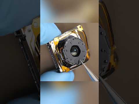
Stacked CMOS image sensors represent a significant advancement in digital imaging technology, offering improved performance and new functionalities compared to traditional CMOS sensors. In a conventional CMOS image sensor, the photodiodes and pixel circuitry are fabricated on a single silicon substrate. In contrast, stacked CMOS image sensors separate the pixel layer (where light is captured) from the logic layer (where signal processing occurs), stacking them vertically and connecting them using advanced techniques such as through-silicon vias (TSVs). This architecture enables each layer to be optimized independently, leading to enhanced image quality, faster readout speeds, and reduced chip size.
The separation of pixel and logic layers allows for the integration of more sophisticated processing circuits, such as high-speed analog-to-digital converters and advanced noise reduction algorithms, directly beneath the pixel array. This not only improves the sensor’s dynamic range and low-light performance but also enables new features like real-time high dynamic range (HDR) imaging and on-chip artificial intelligence (AI) processing. Stacked CMOS sensors are now widely used in smartphones, digital cameras, and automotive applications, where compact size and high performance are critical requirements.
The development and commercialization of stacked CMOS image sensors have been driven by leading semiconductor companies, with Sony Semiconductor Solutions pioneering the technology. As the demand for higher resolution and smarter imaging systems continues to grow, stacked CMOS image sensors are expected to play a central role in the evolution of digital imaging.
How Stacked Architecture Differs from Traditional CMOS Sensors
Stacked CMOS image sensors represent a significant evolution from traditional CMOS sensor architectures, primarily through their innovative use of vertically integrated layers. In conventional CMOS sensors, all pixel circuitry—including photodiodes and signal processing elements—resides on a single silicon substrate. This monolithic approach imposes limitations on pixel size, performance, and the integration of advanced features due to space and process constraints.
In contrast, stacked CMOS image sensors separate the pixel array and the logic circuitry into distinct layers, which are then bonded together using advanced wafer stacking techniques. The top layer typically contains the photodiodes and color filters, optimized solely for light capture, while the bottom layer houses complex signal processing circuits, memory, and sometimes even artificial intelligence accelerators. This separation allows each layer to be manufactured using processes best suited to their function, enabling smaller pixels, higher resolution, and faster readout speeds without compromising image quality or sensor size.
The stacked architecture also facilitates the integration of additional features such as on-chip phase detection autofocus, high dynamic range (HDR) processing, and real-time noise reduction, which are challenging to implement in traditional designs. Furthermore, by reducing the wiring and interconnect length between the pixel and logic layers, stacked sensors achieve lower power consumption and improved signal integrity, resulting in better low-light performance and faster data transfer rates. Leading manufacturers like Sony Semiconductor Solutions have pioneered this technology, making stacked CMOS sensors a cornerstone of modern smartphone and digital camera imaging systems.
Breakthroughs in Image Quality and Processing Speed
Stacked CMOS image sensors have driven significant advancements in both image quality and processing speed, fundamentally transforming digital imaging. By vertically integrating the pixel layer and the logic circuitry on separate substrates, stacked architectures enable the use of advanced signal processing and memory directly beneath the photodiodes. This separation allows for larger, more efficient pixels, which improves light sensitivity and dynamic range, resulting in clearer images with reduced noise, especially in low-light conditions. For example, the implementation of stacked sensor technology in consumer devices has led to notable improvements in color accuracy and detail retention, as demonstrated by Sony Semiconductor Solutions Corporation.
Processing speed has also seen remarkable gains. The stacked design allows for the integration of high-speed DRAM or advanced logic circuits directly under the pixel array, enabling rapid data readout and real-time image processing. This architecture supports features such as ultra-fast autofocus, high frame rate video capture, and reduced rolling shutter distortion. For instance, the use of stacked sensors in smartphones and professional cameras has enabled burst shooting at rates previously unattainable with traditional CMOS sensors, as highlighted by Canon Inc.. Furthermore, the ability to process image data on-chip reduces latency and power consumption, which is critical for mobile and embedded applications.
Overall, stacked CMOS image sensors represent a leap forward in both image quality and processing speed, paving the way for new imaging applications in fields ranging from consumer electronics to automotive and industrial vision systems.
Impact on Smartphone and Consumer Electronics Cameras
Stacked CMOS image sensors have significantly transformed the landscape of smartphone and consumer electronics cameras by enabling higher performance in increasingly compact devices. Unlike traditional sensors, stacked CMOS designs separate the pixel array and the logic circuitry into different layers, which are then vertically integrated. This architecture allows for more advanced signal processing, faster readout speeds, and the integration of additional features directly onto the sensor chip. As a result, smartphones equipped with stacked CMOS sensors can achieve higher resolution, improved low-light performance, and faster autofocus, all within the slim form factors demanded by modern consumer devices.
The impact of stacked CMOS sensors is particularly evident in flagship smartphones, where manufacturers leverage this technology to deliver features such as real-time HDR, multi-frame noise reduction, and high-speed video capture. For instance, the adoption of stacked sensor technology has enabled burst shooting at up to 20 frames per second and 4K video recording at high frame rates, capabilities that were previously limited to dedicated cameras. Furthermore, the increased processing power on the sensor itself reduces the load on the main application processor, leading to more efficient power consumption and longer battery life—an essential consideration for mobile devices.
Major industry players, including Sony Semiconductor Solutions and Samsung Semiconductor, have been at the forefront of stacked CMOS sensor development, driving innovation in computational photography and enabling new user experiences such as advanced portrait modes and AI-powered scene recognition. As consumer expectations for camera performance continue to rise, stacked CMOS image sensors are poised to remain a cornerstone technology in the evolution of mobile and consumer imaging devices.
Enabling Advanced Features: High Dynamic Range, Low-Light Performance, and AI Integration
Stacked CMOS image sensors have revolutionized the capabilities of modern imaging systems by enabling advanced features such as high dynamic range (HDR), superior low-light performance, and seamless integration of artificial intelligence (AI) processing. The stacked architecture separates the pixel array and the logic circuitry into different layers, interconnected through high-density vertical connections. This design allows for the inclusion of more sophisticated signal processing and memory directly beneath the pixel layer, without increasing the sensor’s footprint.
For HDR imaging, stacked sensors can capture multiple exposures simultaneously or in rapid succession, thanks to the high-speed readout enabled by the dedicated logic layer. This results in images with greater detail in both bright and dark areas, surpassing the capabilities of traditional single-layer sensors. Enhanced low-light performance is achieved by optimizing the pixel structure and reducing noise through on-chip processing, which is more feasible in a stacked configuration. The proximity of advanced analog-to-digital converters and noise reduction circuits to the pixel layer minimizes signal degradation, leading to clearer images in challenging lighting conditions.
Furthermore, the integration of AI accelerators within the logic layer of stacked CMOS sensors allows for real-time image analysis, such as object detection, scene recognition, and autofocus adjustments, directly on the sensor. This not only reduces latency but also offloads processing from the main device processor, enabling smarter and more efficient imaging applications. Leading manufacturers like Sony Semiconductor Solutions and Samsung Semiconductor have demonstrated these advancements, setting new standards for mobile, automotive, and industrial imaging systems.
Manufacturing Challenges and Industry Adoption
The manufacturing of stacked CMOS image sensors presents unique challenges compared to traditional front- or back-illuminated CMOS sensors. Stacked architectures require the precise alignment and bonding of multiple silicon wafers—typically separating the pixel array from the logic circuitry. This process, known as wafer-to-wafer or die-to-wafer bonding, demands sub-micron accuracy to ensure electrical connectivity and image quality. Achieving such precision at scale increases complexity and cost, as even minor misalignments can lead to yield loss or degraded sensor performance. Additionally, the thinning of wafers to facilitate stacking introduces fragility, necessitating advanced handling and inspection techniques throughout the production line.
Another significant challenge is thermal management. The close proximity of logic and pixel layers can lead to localized heating, potentially affecting sensor noise and reliability. Manufacturers must therefore integrate effective heat dissipation solutions without compromising the compactness that stacked designs offer. Furthermore, the integration of through-silicon vias (TSVs) for vertical interconnects adds further process steps and requires careful optimization to avoid crosstalk and maintain signal integrity.
Despite these hurdles, industry adoption of stacked CMOS image sensors has accelerated, driven by the demand for higher performance in compact devices such as smartphones and automotive cameras. Leading companies like Sony Semiconductor Solutions Corporation and Samsung Electronics have pioneered mass production, leveraging proprietary bonding and miniaturization technologies. As manufacturing techniques mature and economies of scale improve, stacked CMOS sensors are expected to become the standard for high-end imaging applications, further pushing the boundaries of sensor performance and device integration.
Future Trends: Beyond Smartphones—Automotive, Security, and Industrial Applications
Stacked CMOS image sensors, initially developed to meet the demanding requirements of smartphone photography, are now poised to revolutionize a range of industries beyond consumer electronics. In the automotive sector, these sensors are being integrated into advanced driver-assistance systems (ADAS) and autonomous vehicles, where their high dynamic range, low noise, and rapid readout capabilities enable more reliable object detection and situational awareness under challenging lighting conditions. Leading automotive suppliers are already collaborating with sensor manufacturers to develop custom stacked CMOS solutions tailored for in-cabin monitoring and surround-view systems (Sony Semiconductor Solutions Corporation).
In security and surveillance, stacked CMOS sensors offer significant advantages, such as improved low-light performance and faster frame rates, which are critical for real-time monitoring and facial recognition. The ability to integrate on-chip artificial intelligence (AI) processing within the sensor stack further enhances their utility, enabling edge analytics and reducing the need for high-bandwidth data transmission to centralized servers (ams OSRAM).
Industrial applications are also benefiting from the evolution of stacked CMOS technology. In machine vision, robotics, and quality control, these sensors provide higher resolution and faster data throughput, supporting more precise inspection and automation tasks. The trend toward miniaturization and integration of additional functions—such as depth sensing and spectral imaging—within the sensor stack is expected to drive further adoption across these sectors (onsemi).
As stacked CMOS image sensors continue to evolve, their impact is set to expand well beyond smartphones, enabling smarter, safer, and more efficient systems across automotive, security, and industrial domains.
Conclusion: The Road Ahead for Stacked CMOS Image Sensors
Stacked CMOS image sensors have rapidly evolved from a novel concept to a cornerstone technology in modern imaging systems. Their layered architecture, which separates the photodiode and circuitry into distinct tiers, has enabled significant advancements in pixel miniaturization, readout speed, and power efficiency. As the demand for high-performance imaging in smartphones, automotive systems, and industrial applications continues to grow, stacked CMOS sensors are poised to play an even more critical role in the future of digital imaging.
Looking ahead, ongoing research is focused on further reducing pixel size while maintaining or improving sensitivity and dynamic range. Innovations such as the integration of artificial intelligence processing directly onto the sensor stack and the use of advanced materials for enhanced quantum efficiency are on the horizon. These developments promise to unlock new functionalities, such as real-time computational photography and advanced machine vision capabilities, directly at the sensor level.
However, challenges remain, including the complexity of manufacturing multi-layered structures and ensuring high yield and reliability at scale. Industry leaders are investing in new fabrication techniques and design methodologies to address these hurdles. As these technologies mature, stacked CMOS image sensors are expected to become even more ubiquitous, driving the next wave of innovation in imaging across diverse sectors. For a comprehensive overview of current trends and future directions, see resources from Sony Semiconductor Solutions Corporation and Canon Inc..
Sources & References