How Silicon Photonic Interconnects Are Transforming Data Centers in 2025: Unleashing Unprecedented Bandwidth, Efficiency, and Scalability for the Next Generation of Cloud Infrastructure
- Executive Summary: 2025 Market Snapshot and Key Trends
- Technology Overview: Fundamentals of Silicon Photonic Interconnects
- Current Market Size and 2025–2030 Growth Forecasts
- Key Players and Ecosystem: Leading Companies and Industry Alliances
- Performance Advantages: Bandwidth, Latency, and Energy Efficiency
- Integration with Data Center Architectures: Challenges and Solutions
- Manufacturing Innovations and Cost Reduction Strategies
- Regulatory, Standards, and Interoperability Landscape
- Emerging Applications: AI, HPC, and Cloud-Scale Deployments
- Future Outlook: Market Growth Drivers, Barriers, and Strategic Opportunities
- Sources & References
Executive Summary: 2025 Market Snapshot and Key Trends
In 2025, silicon photonic interconnects are positioned at the forefront of data center innovation, driven by the exponential growth in cloud computing, artificial intelligence (AI), and high-performance computing (HPC) workloads. The demand for higher bandwidth, lower latency, and improved energy efficiency is accelerating the adoption of silicon photonics as a replacement for traditional copper-based and legacy optical interconnects. Major hyperscale data center operators and network equipment manufacturers are actively deploying and scaling silicon photonic solutions to address the limitations of electrical interconnects at data rates of 400G, 800G, and beyond.
Key industry leaders such as Intel Corporation, Cisco Systems, and Inphi (now part of Marvell Technology) are investing heavily in silicon photonics R&D and product commercialization. Intel Corporation has announced volume shipments of 400G and 800G silicon photonic transceivers, targeting hyperscale data centers and cloud providers. Cisco Systems is integrating silicon photonics into its next-generation switches and routers, aiming to deliver higher port densities and lower power consumption. Marvell Technology (following its acquisition of Inphi) is advancing coherent DSP and silicon photonic platform integration for high-speed optical modules.
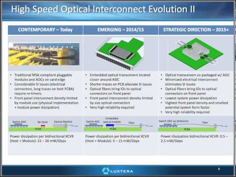
The transition to co-packaged optics (CPO) is a defining trend for 2025 and the coming years. CPO integrates optical engines directly with switch ASICs, reducing electrical signal loss and power consumption. Industry consortia such as the Optical Internetworking Forum (OIF) and Open Compute Project (OCP) are standardizing CPO architectures and interoperability, with pilot deployments expected in leading-edge data centers. The move toward 1.6T and 3.2T optical interconnects is underway, with silicon photonics seen as the enabling technology for these ultra-high-speed links.
In terms of market outlook, the adoption of silicon photonic interconnects is expected to accelerate through 2025 and beyond, as data center operators seek to overcome the physical and economic constraints of copper and legacy optics. The ecosystem is expanding, with new entrants such as Ayar Labs and Rockley Photonics developing advanced optical I/O and sensing solutions. As manufacturing yields improve and costs decline, silicon photonics is poised to become the default interconnect technology for next-generation data centers, supporting the relentless growth in data traffic and compute density.
Technology Overview: Fundamentals of Silicon Photonic Interconnects
Silicon photonic interconnects represent a transformative technology for data center communications, leveraging the optical properties of silicon to transmit data at high speeds with reduced power consumption and increased bandwidth density. At their core, these interconnects utilize integrated photonic circuits fabricated on silicon wafers, enabling the manipulation and transmission of light signals alongside or in place of traditional electrical signals. The fundamental building blocks include silicon-based modulators, photodetectors, waveguides, and multiplexers, all of which can be manufactured using mature CMOS processes, allowing for cost-effective mass production and integration with existing electronic components.
In 2025, the deployment of silicon photonic interconnects in data centers is accelerating, driven by the exponential growth in cloud computing, artificial intelligence, and high-performance computing workloads. Traditional copper-based interconnects are increasingly limited by bandwidth, signal integrity, and energy efficiency constraints, especially over distances greater than a few meters. Silicon photonics addresses these challenges by enabling optical links that support data rates of 400 Gbps and beyond per channel, with ongoing demonstrations of 800 Gbps and 1.6 Tbps solutions on the horizon.
Key to the technology’s adoption is the ability to integrate photonic and electronic components on a single chip or within a single package. This integration reduces latency, power consumption, and physical footprint, all critical factors for hyperscale data centers. Companies such as Intel Corporation have been at the forefront, commercializing silicon photonic transceivers and co-packaged optics for switch and server interconnects. Cisco Systems, Inc. and Broadcom Inc. are also actively developing and deploying silicon photonic solutions, with a focus on pluggable and co-packaged optical modules for next-generation data center architectures.
The technology relies on the use of wavelength-division multiplexing (WDM), allowing multiple data streams to be transmitted simultaneously over a single fiber, further increasing aggregate bandwidth. Silicon photonic devices are also being designed for compatibility with emerging standards such as 800G and 1.6T Ethernet, ensuring future-proof scalability. Industry organizations like the Optical Internetworking Forum (OIF) and Ethernet Alliance are actively working to standardize interfaces and interoperability, which is expected to accelerate adoption in the coming years.
Looking ahead, the outlook for silicon photonic interconnects in data centers is robust. As manufacturing yields improve and integration with advanced packaging technologies matures, costs are expected to decline, making the technology accessible for a broader range of applications. The convergence of photonics and electronics at the chip and system level is poised to become a foundational element of data center infrastructure, supporting the relentless demand for higher bandwidth, lower latency, and improved energy efficiency.
Current Market Size and 2025–2030 Growth Forecasts
The market for silicon photonic interconnects in data centers is experiencing robust growth, driven by the exponential increase in data traffic, the proliferation of artificial intelligence (AI) workloads, and the need for higher bandwidth and energy efficiency. As of 2025, silicon photonics has moved from early adoption to a more mainstream role in hyperscale and cloud data centers, with leading technology companies and component manufacturers ramping up production and deployment.
Major industry players such as Intel Corporation, Cisco Systems, and Inphi (now part of Marvell Technology) have made significant investments in silicon photonics, with Intel reporting shipment of millions of silicon photonic transceivers to cloud and communication service providers. These transceivers are now widely used for 100G, 200G, and 400G optical links, and the transition to 800G and even 1.6T is underway, with product announcements and pilot deployments expected to accelerate through 2025 and beyond.
The current global market size for silicon photonic interconnects in data centers is estimated to be in the multi-billion dollar range in 2025, with double-digit annual growth rates projected through 2030. This growth is fueled by the adoption of co-packaged optics, which integrate photonic and electronic components in a single package, reducing power consumption and enabling higher data rates. Companies such as Intel Corporation and Broadcom Inc. are actively developing co-packaged optical solutions, with prototypes and early commercial products targeting next-generation data center switches.
The outlook for 2025–2030 suggests that silicon photonic interconnects will become increasingly critical for data center scalability. Hyperscale operators, including Microsoft and Google, are collaborating with component suppliers to accelerate the deployment of silicon photonics in their infrastructure, aiming to support AI clusters and high-performance computing workloads. Industry organizations such as the Optical Internetworking Forum (OIF) and Open Compute Project (OCP) are also driving standardization efforts, which are expected to further catalyze market growth and interoperability.
By 2030, silicon photonic interconnects are projected to dominate new data center builds, with widespread adoption of 800G and 1.6T links, and increasing integration of photonics at the chip and package level. The market is expected to see continued innovation in packaging, integration, and manufacturing, with established players and new entrants alike competing to deliver higher performance, lower cost, and greater energy efficiency.
Key Players and Ecosystem: Leading Companies and Industry Alliances
The silicon photonic interconnect ecosystem for data centers in 2025 is characterized by a dynamic interplay of established technology giants, innovative startups, foundries, and industry alliances. These entities are collectively driving the commercialization and deployment of high-speed, energy-efficient optical interconnects to meet the surging bandwidth and power efficiency demands of hyperscale and enterprise data centers.
Among the most prominent players, Intel Corporation stands out as a pioneer and market leader in silicon photonics. Intel’s pluggable transceivers and co-packaged optics (CPO) solutions are already deployed in large-scale data centers, with the company announcing 1.6 Tbps optical modules and demonstrating integrated photonic engines for next-generation switches. Cisco Systems is another major force, leveraging its acquisition of Luxtera to integrate silicon photonics into its networking equipment, targeting both pluggable and on-board optical interconnects.
Other key contributors include Ayar Labs, a startup specializing in chip-to-chip optical I/O using monolithic integration, and Rockley Photonics, which focuses on high-density optical interconnects and sensing. Inphi Corporation (now part of Marvell Technology) is recognized for its high-speed optical DSPs and silicon photonics platforms, while Coherent Corp. (formerly II-VI Incorporated) supplies photonic integrated circuits and transceivers for hyperscale data centers.
Foundries and manufacturing partners play a crucial role in scaling production. GLOBALFOUNDRIES and Taiwan Semiconductor Manufacturing Company (TSMC) offer silicon photonics process technologies to fabless companies, enabling volume manufacturing of photonic integrated circuits (PICs). Advanced Micro Devices (AMD) and NVIDIA Corporation are also investing in photonic interconnects for AI and high-performance computing, with NVIDIA’s acquisition of Mellanox and AMD’s acquisition of Xilinx expanding their capabilities in optical networking.
Industry alliances and standards bodies are essential for ecosystem cohesion and interoperability. The Optical Internetworking Forum (OIF) and Co-Packaged Optics Collaboration (COBO) are actively developing standards for CPO, optical engines, and pluggable modules. The Open Compute Project (OCP) fosters collaboration among hyperscalers, equipment vendors, and component suppliers to accelerate adoption of open, interoperable silicon photonic solutions.
Looking ahead, the ecosystem is expected to see intensified collaboration between chipmakers, foundries, and system integrators, with a focus on scaling to 1.6 Tbps and beyond, reducing power consumption, and enabling new architectures such as optical circuit switching and disaggregated data center fabrics. The convergence of AI, cloud, and edge computing will further drive demand for advanced silicon photonic interconnects, positioning these key players and alliances at the forefront of data center innovation through the latter half of the decade.
Performance Advantages: Bandwidth, Latency, and Energy Efficiency
Silicon photonic interconnects are rapidly emerging as a transformative technology for data center networks, offering significant performance advantages over traditional electrical interconnects in terms of bandwidth, latency, and energy efficiency. As data centers scale to meet the demands of artificial intelligence (AI), cloud computing, and high-performance workloads, the limitations of copper-based connections—such as signal attenuation, electromagnetic interference, and high power consumption—have become increasingly apparent.
In 2025, silicon photonics is enabling data centers to achieve unprecedented bandwidth densities. State-of-the-art silicon photonic transceivers are now delivering per-lane data rates of 100 Gbps and beyond, with aggregate module capacities reaching 800 Gbps and 1.6 Tbps. These advances are being driven by leading manufacturers such as Intel, which has commercialized silicon photonics modules for hyperscale data centers, and Cisco Systems, which integrates silicon photonics into its networking platforms. The use of wavelength division multiplexing (WDM) on silicon photonic chips allows multiple data streams to be transmitted simultaneously over a single fiber, further multiplying bandwidth without increasing physical footprint.
Latency is another critical metric for data center interconnects, especially for distributed AI training and real-time analytics. Silicon photonic links offer lower latency compared to electrical interconnects, primarily due to the elimination of signal conversions and the ability to transmit data over longer distances without repeaters. Companies like Inphi (now part of Marvell Technology) and Ayar Labs are pioneering low-latency optical I/O solutions, with Ayar Labs demonstrating chip-to-chip optical connections that reduce serialization and deserialization delays, a key bottleneck in traditional architectures.
Energy efficiency is a major driver for the adoption of silicon photonics in data centers. Optical interconnects consume significantly less power per bit transmitted compared to copper, especially at higher data rates and longer distances. For example, Intel reports that its silicon photonic transceivers can reduce power consumption by up to 50% compared to legacy solutions. This reduction is crucial as data centers face mounting pressure to control operational costs and meet sustainability targets.
Looking ahead, the industry expects further improvements in performance as silicon photonics technology matures. Integration of lasers, modulators, and detectors on a single silicon die is anticipated to drive down costs and further enhance energy efficiency. With ongoing investments from major players such as Intel, Cisco Systems, and Marvell Technology, silicon photonic interconnects are poised to become the backbone of next-generation data center architectures, supporting the exponential growth in data traffic projected for the coming years.
Integration with Data Center Architectures: Challenges and Solutions
The integration of silicon photonic interconnects into data center architectures is accelerating in 2025, driven by the need for higher bandwidth, lower latency, and improved energy efficiency. However, this transition presents several technical and operational challenges that industry leaders are actively addressing.
One of the primary challenges is the seamless integration of silicon photonics with existing CMOS-based electronics. Silicon photonic devices, such as modulators and detectors, must be co-packaged with electronic ASICs to minimize signal loss and power consumption. This co-packaging requires advanced manufacturing processes and precise alignment, which has led to significant investments by major players. Intel Corporation has been at the forefront, developing co-packaged optics (CPO) solutions that integrate photonic and electronic components on a single substrate, aiming to deliver terabit-scale connectivity for next-generation data centers.
Thermal management is another critical issue. Silicon photonic devices are sensitive to temperature fluctuations, which can affect performance and reliability. Data center operators are exploring new cooling techniques and materials to maintain optimal operating conditions. Companies like Cisco Systems, Inc. are collaborating with partners to develop advanced thermal solutions that ensure the stability of photonic interconnects in dense server environments.
Interoperability and standardization also pose challenges. The rapid evolution of photonic technologies has led to a fragmented ecosystem, with varying interface standards and form factors. Industry consortia such as the Optical Internetworking Forum (OIF) and the Open Compute Project (OCP) are working to establish common specifications for optical modules and interfaces, facilitating broader adoption and multi-vendor compatibility.
On the solutions front, hyperscale data center operators are piloting and deploying silicon photonic interconnects in high-performance computing clusters and AI workloads, where traditional copper-based links are reaching their physical limits. Advanced Micro Devices, Inc. (AMD) and NVIDIA Corporation are integrating photonic interconnects into their server platforms to support the massive data throughput required by modern AI and machine learning applications.
Looking ahead, the outlook for silicon photonic integration in data centers is promising. As manufacturing yields improve and costs decline, broader deployment is expected over the next few years. The convergence of photonics and electronics is set to redefine data center architectures, enabling scalable, energy-efficient, and high-bandwidth networks that can meet the demands of future digital infrastructure.
Manufacturing Innovations and Cost Reduction Strategies
The manufacturing landscape for silicon photonic interconnects in data centers is undergoing rapid transformation as the industry seeks to address both scalability and cost challenges. In 2025, several key innovations are converging to make silicon photonics more viable for large-scale deployment, with a focus on advanced integration techniques, streamlined packaging, and leveraging existing CMOS fabrication infrastructure.
One of the most significant trends is the adoption of wafer-scale integration, which allows for the simultaneous fabrication of photonic and electronic components on a single silicon substrate. This approach reduces assembly complexity and improves yield, directly impacting cost per bit. Leading manufacturers such as Intel Corporation have invested heavily in monolithic integration, enabling the co-packaging of photonic transceivers with switch ASICs. This not only minimizes optical losses but also reduces the footprint and power consumption of interconnect modules.
Another area of innovation is the development of advanced packaging solutions. Traditional fiber array and connectorization methods are being replaced by automated, high-precision alignment and bonding techniques. Companies like Ayar Labs are pioneering chiplet-based architectures, where photonic I/O chiplets are integrated alongside electronic processors using standard interposers. This modular approach streamlines manufacturing and supports rapid scaling to higher data rates, such as 800G and beyond.
Cost reduction is further driven by the use of mature CMOS foundries for photonic device fabrication. By leveraging the same high-volume manufacturing processes used for electronic ICs, suppliers can achieve economies of scale and consistent quality. GlobalFoundries and Taiwan Semiconductor Manufacturing Company (TSMC) have both expanded their silicon photonics process offerings, enabling fabless companies to bring new designs to market without the need for dedicated photonics fabs.
Looking ahead, the industry is also exploring heterogeneous integration, where materials such as indium phosphide (InP) or silicon nitride are combined with silicon to enhance performance while maintaining cost advantages. Collaborative efforts between device manufacturers and data center operators are expected to accelerate the adoption of these technologies, with hyperscale cloud providers playing a pivotal role in setting requirements and driving volume.
Overall, the next few years will likely see continued progress in manufacturing efficiency and cost reduction, making silicon photonic interconnects increasingly attractive for mainstream data center deployments. The combination of wafer-scale integration, advanced packaging, and CMOS compatibility is poised to deliver the scalability and affordability required for the next generation of high-speed, energy-efficient data center networks.
Regulatory, Standards, and Interoperability Landscape
The regulatory, standards, and interoperability landscape for silicon photonic interconnects in data centers is rapidly evolving as the technology matures and adoption accelerates through 2025 and beyond. The industry’s focus is on ensuring seamless integration, high performance, and multi-vendor compatibility, which are critical for hyperscale and enterprise data center operators.
Key standards bodies such as the IEEE and the Optical Internetworking Forum (OIF) are at the forefront of defining specifications for next-generation optical interconnects. The IEEE 802.3 working group continues to develop and refine standards for Ethernet-based optical modules, including 400G, 800G, and emerging 1.6T interfaces, which are increasingly being implemented using silicon photonics. The OIF, meanwhile, is driving interoperability through implementation agreements for coherent and pluggable optics, such as the 400ZR and 800ZR standards, which are directly relevant to silicon photonic transceivers.
Interoperability testing events, such as OIF’s ongoing plugfests, have become crucial for validating multi-vendor compatibility of silicon photonic modules. These events bring together leading manufacturers—including Intel, Cisco Systems, Inphi (now part of Marvell Technology), and Ayar Labs—to demonstrate compliance with standards and ensure that products can be deployed interchangeably in large-scale data center environments.
The Connectivity Standards Alliance and the Storage Networking Industry Association (SNIA) are also contributing to the ecosystem by developing management protocols and interface definitions that support the integration of silicon photonic devices into broader data center architectures. These efforts are complemented by the Compute Express Link (CXL) Consortium, which is exploring photonic interconnects for memory and accelerator expansion, further broadening the regulatory and standards landscape.
On the regulatory front, compliance with international safety and electromagnetic compatibility (EMC) requirements remains essential. Organizations such as the International Electrotechnical Commission (IEC) and International Telecommunication Union (ITU) provide guidelines for optical component safety, laser emissions, and environmental standards, which manufacturers must adhere to as silicon photonics moves into mass deployment.
Looking ahead, the convergence of standards for co-packaged optics, advanced modulation formats, and energy-efficient designs is expected to accelerate. Industry collaboration through multi-source agreements (MSAs) and open standards initiatives will be pivotal in ensuring that silicon photonic interconnects deliver on their promise of scalable, interoperable, and sustainable data center connectivity through the remainder of the decade.
Emerging Applications: AI, HPC, and Cloud-Scale Deployments
The rapid expansion of artificial intelligence (AI), high-performance computing (HPC), and cloud-scale deployments is driving a paradigm shift in data center architectures, with silicon photonic interconnects emerging as a critical enabling technology. As data centers face unprecedented demands for bandwidth, energy efficiency, and scalability, traditional copper-based interconnects are increasingly unable to meet the requirements of next-generation workloads. Silicon photonics, leveraging the integration of optical components onto silicon chips, offers a compelling solution by delivering high-speed, low-latency, and energy-efficient data transmission.
In 2025, hyperscale cloud providers and AI infrastructure builders are accelerating the adoption of silicon photonic interconnects to support the explosive growth of large language models, generative AI, and data-intensive HPC applications. Companies such as Intel Corporation and NVIDIA Corporation are at the forefront, with Intel’s co-packaged optics and photonic transceivers being deployed in next-generation server and switch platforms, and NVIDIA integrating silicon photonics into its advanced networking solutions for AI clusters. Cisco Systems, Inc. is also investing in silicon photonics for its data center switching and interconnect products, aiming to address the growing need for scalable, high-bandwidth connectivity.
The transition to 800G and 1.6T optical modules, enabled by silicon photonics, is underway, with major suppliers such as Inphi (now part of Marvell Technology, Inc.) and Ayar Labs delivering pluggable and co-packaged solutions tailored for AI and cloud-scale environments. These modules are designed to reduce power consumption per bit and increase port density, which are essential for the massive scale-out of GPU and accelerator clusters. Ayar Labs, in particular, is pioneering optical I/O for chip-to-chip and chip-to-module interconnects, targeting the bottlenecks in AI training fabrics.
Industry alliances and standards bodies, such as the Optical Internetworking Forum (OIF) and Open Compute Project Foundation, are actively defining interoperability standards and reference architectures to accelerate the deployment of silicon photonic technologies in hyperscale data centers. These collaborative efforts are expected to drive down costs and ensure multi-vendor compatibility, further catalyzing adoption.
Looking ahead, the outlook for silicon photonic interconnects in AI, HPC, and cloud-scale deployments is robust. As data center operators prioritize energy efficiency and performance, silicon photonics is poised to become a foundational technology, enabling the next wave of innovation in distributed AI training, exascale computing, and elastic cloud services. The next few years will likely see broader commercialization, deeper integration into server and switch architectures, and the emergence of new applications leveraging the unique advantages of silicon photonics.
Future Outlook: Market Growth Drivers, Barriers, and Strategic Opportunities
The outlook for silicon photonic interconnects in data centers through 2025 and the following years is shaped by a convergence of technological, economic, and strategic factors. As hyperscale data centers and cloud service providers face exponential growth in data traffic, the demand for high-bandwidth, energy-efficient, and cost-effective interconnect solutions is intensifying. Silicon photonics, which integrates optical components onto silicon chips, is increasingly recognized as a key enabler for next-generation data center architectures.
Market Growth Drivers
- Bandwidth and Power Efficiency: The transition to 400G, 800G, and emerging 1.6T optical transceivers is accelerating, driven by the need to support AI/ML workloads and high-density server architectures. Silicon photonics offers significant advantages in bandwidth density and power consumption compared to traditional copper or direct-detect optics, making it attractive for large-scale deployments.
- Manufacturing Scalability: The compatibility of silicon photonics with CMOS fabrication processes enables mass production and cost reduction, which is critical for widespread adoption. Industry leaders such as Intel Corporation and Cisco Systems, Inc. are investing heavily in silicon photonics R&D and manufacturing, aiming to deliver scalable solutions for hyperscale and enterprise data centers.
- Integration and Co-Packaging: The trend toward co-packaged optics—integrating optical engines with switch ASICs—promises to further reduce power consumption and latency. Companies like Broadcom Inc. and Advanced Micro Devices, Inc. (AMD) are actively developing co-packaged solutions, anticipating commercial deployments in the next few years.
Barriers to Adoption
- Technical Complexity: Integrating photonic and electronic components at scale presents significant engineering challenges, including thermal management, packaging, and testing. Ensuring reliability and interoperability across multi-vendor environments remains a hurdle.
- Initial Investment: While silicon photonics promises long-term cost savings, the upfront investment in new manufacturing lines, packaging technologies, and workforce training can be substantial, particularly for smaller players.
Strategic Opportunities
- Vertical Integration: Major cloud providers and hyperscalers are increasingly pursuing in-house silicon photonics development to optimize performance and control supply chains. Google LLC and Microsoft Corporation are reported to be investing in custom photonic interconnects for their data center infrastructure.
- Open Standards and Ecosystem Collaboration: Industry consortia such as the Optical Internetworking Forum (OIF) are driving standardization efforts, which will be crucial for interoperability and accelerating market adoption.
Looking ahead, the silicon photonics market for data center interconnects is poised for robust growth, propelled by the relentless demand for bandwidth and efficiency. Strategic investments, ecosystem collaboration, and continued innovation will be key to overcoming technical and economic barriers, positioning silicon photonics as a foundational technology for the data centers of the future.
Sources & References
- Cisco Systems
- Inphi (now part of Marvell Technology)
- Marvell Technology
- Optical Internetworking Forum (OIF)
- Open Compute Project (OCP)
- Ayar Labs
- Rockley Photonics
- Broadcom Inc.
- Ethernet Alliance
- Microsoft
- NVIDIA Corporation
- IEEE
- International Telecommunication Union