
Extreme Ultraviolet Lithography Metrology Market Report 2025: In-Depth Analysis of Growth Drivers, Technology Innovations, and Global Forecasts. Explore Key Trends, Competitive Dynamics, and Strategic Opportunities Shaping the Industry.
- Executive Summary and Market Overview
- Key Technology Trends in EUV Lithography Metrology
- Competitive Landscape and Leading Players
- Market Growth Forecasts and Revenue Projections (2025–2030)
- Regional Analysis: North America, Europe, Asia-Pacific, and Rest of World
- Challenges, Risks, and Market Entry Barriers
- Opportunities and Strategic Recommendations
- Future Outlook: Emerging Applications and Long-Term Trends
- Sources & References
Executive Summary and Market Overview
Extreme Ultraviolet (EUV) Lithography Metrology is a critical segment within the semiconductor manufacturing industry, providing the measurement and inspection solutions necessary to ensure the precision and yield of EUV lithography processes. As chipmakers push towards sub-5nm nodes, the demand for advanced metrology tools capable of handling the unique challenges of EUV—such as shorter wavelengths, higher sensitivity to defects, and complex mask structures—has intensified. The global EUV lithography metrology market is projected to experience robust growth through 2025, driven by the rapid adoption of EUV lithography in high-volume manufacturing by leading foundries and integrated device manufacturers (IDMs).
According to industry analyses, the market for EUV lithography metrology is expected to reach a valuation of over USD 1.2 billion by 2025, growing at a compound annual growth rate (CAGR) exceeding 10% from 2022 to 2025. This growth is underpinned by the increasing capital expenditures of semiconductor manufacturers such as TSMC, Samsung Electronics, and Intel, all of whom are ramping up EUV capacity to meet the surging demand for advanced logic and memory chips.
Key players in the EUV metrology space include ASML Holding, which not only dominates EUV lithography tool supply but also offers integrated metrology solutions, as well as specialized metrology providers such as KLA Corporation and Hitachi High-Tech. These companies are investing heavily in R&D to address the metrology challenges posed by EUV, including overlay accuracy, critical dimension (CD) measurement, and defect inspection at the nanometer scale.
Geographically, Asia-Pacific remains the largest and fastest-growing market for EUV lithography metrology, fueled by aggressive fab expansions in Taiwan, South Korea, and China. North America and Europe also contribute significantly, with ongoing investments in advanced semiconductor R&D and manufacturing infrastructure.
In summary, the EUV lithography metrology market in 2025 is characterized by rapid technological innovation, strong capital investment, and a highly competitive landscape. The sector’s growth is intrinsically linked to the broader adoption of EUV lithography, which is now a cornerstone technology for next-generation semiconductor devices. As the industry continues to scale down feature sizes, the importance of precise and reliable metrology solutions will only intensify, ensuring continued market expansion and technological advancement.
Key Technology Trends in EUV Lithography Metrology
Extreme Ultraviolet (EUV) lithography metrology is undergoing rapid technological evolution as semiconductor manufacturers push toward sub-5nm nodes and beyond. In 2025, several key technology trends are shaping the metrology landscape, driven by the need for higher precision, throughput, and integration with advanced process control systems.
- Increased Adoption of In-Line and In-Situ Metrology: To minimize process variability and maximize yield, chipmakers are increasingly integrating metrology tools directly into EUV lithography lines. In-line and in-situ metrology solutions enable real-time monitoring of critical parameters such as overlay, critical dimension (CD), and focus, reducing feedback loops and improving process control. Companies like ASML are advancing integrated metrology modules that work seamlessly with EUV scanners.
- Advancements in Scatterometry and Hybrid Metrology: Scatterometry, a non-destructive optical technique, is being enhanced with machine learning algorithms and combined with other methods (such as CD-SEM and AFM) to form hybrid metrology solutions. This approach improves measurement accuracy for complex EUV patterns, especially as feature sizes shrink and 3D structures become more prevalent. KLA Corporation and Hitachi High-Tech are leading providers of such hybrid metrology platforms.
- High-Resolution, Low-Damage Electron Microscopy: As EUV features approach atomic scales, advanced electron microscopy tools with low-voltage operation are being deployed to minimize sample damage while providing high-resolution imaging. These tools are essential for defect review and root-cause analysis in EUV processes.
- AI-Driven Data Analytics and Predictive Metrology: The integration of artificial intelligence and big data analytics is transforming metrology by enabling predictive maintenance, anomaly detection, and process optimization. AI-driven platforms can analyze vast datasets from multiple metrology sources, providing actionable insights for yield improvement. Applied Materials and Synopsys are investing in such data-centric metrology solutions.
- Metrology for Stochastic Defects and EUV-Specific Challenges: Addressing stochastic defects—random, pattern-dependent errors unique to EUV—requires new metrology techniques capable of high sensitivity and statistical analysis across large wafer areas. The industry is developing specialized inspection tools to detect and characterize these defects, as highlighted in recent SEMI reports.
These technology trends are critical for enabling the continued scaling of semiconductor devices and ensuring the manufacturability of next-generation chips using EUV lithography in 2025 and beyond.
Competitive Landscape and Leading Players
The competitive landscape of the Extreme Ultraviolet (EUV) Lithography Metrology market in 2025 is characterized by a concentrated group of global players, each leveraging advanced technology portfolios and strategic partnerships to maintain or expand their market share. The market is primarily driven by the increasing adoption of EUV lithography in semiconductor manufacturing, particularly for nodes below 7nm, which necessitates highly precise metrology solutions.
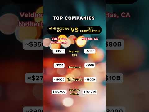
Key players dominating the EUV lithography metrology segment include ASML Holding NV, KLA Corporation, Hitachi High-Tech Corporation, and Carl Zeiss AG. These companies have established themselves as leaders through significant investments in R&D, proprietary metrology technologies, and close collaborations with major semiconductor foundries.
- ASML Holding NV remains the undisputed leader in EUV lithography equipment and has expanded its metrology offerings through integrated solutions that enhance overlay and critical dimension (CD) measurement accuracy. ASML’s holistic approach, combining lithography and metrology, provides a competitive edge, especially as chipmakers demand tighter process control for advanced nodes (ASML Holding NV).
- KLA Corporation is a major supplier of standalone metrology and inspection systems tailored for EUV processes. Its portfolio includes advanced optical and e-beam metrology tools, which are critical for defect detection and process optimization in high-volume manufacturing (KLA Corporation).
- Hitachi High-Tech Corporation specializes in CD-SEM (Critical Dimension Scanning Electron Microscope) systems, which are widely adopted for EUV mask and wafer inspection. The company’s focus on high-resolution, low-damage metrology tools has strengthened its position in the market (Hitachi High-Tech Corporation).
- Carl Zeiss AG provides high-precision optics and metrology solutions, particularly for EUV mask inspection and repair. Its collaboration with ASML on EUV optics and metrology modules is a key differentiator (Carl Zeiss AG).
The competitive environment is further shaped by ongoing innovation, with players investing in AI-driven analytics, in-line metrology, and next-generation inspection technologies. Strategic alliances between equipment vendors and semiconductor manufacturers are expected to intensify, as the industry seeks to overcome the technical challenges of EUV process control and yield enhancement.
Market Growth Forecasts and Revenue Projections (2025–2030)
The Extreme Ultraviolet (EUV) Lithography Metrology market is poised for robust growth between 2025 and 2030, driven by the accelerating adoption of EUV lithography in advanced semiconductor manufacturing. As chipmakers transition to sub-7nm and 5nm nodes, the demand for precise metrology solutions to monitor and control EUV processes is intensifying. According to projections by Gartner, the global semiconductor equipment market, which includes EUV metrology tools, is expected to maintain a compound annual growth rate (CAGR) of approximately 8% through 2030, with EUV-specific segments outpacing the broader market due to their critical role in next-generation chip fabrication.
Revenue for the EUV lithography metrology segment is forecasted to reach between $1.2 billion and $1.5 billion by 2025, with continued double-digit growth anticipated through 2030. This expansion is underpinned by significant investments from leading foundries such as TSMC, Samsung Electronics, and Intel, all of which are scaling up EUV capacity and, consequently, their metrology infrastructure. SEMI reports that capital expenditures on EUV-related metrology equipment are expected to grow at a CAGR of 12–15% over the forecast period, reflecting the increasing complexity and tighter process control requirements of EUV lithography.
Key market drivers include the proliferation of AI, 5G, and high-performance computing applications, which necessitate advanced chips manufactured with EUV technology. As a result, metrology vendors such as KLA Corporation and ASML are expanding their product portfolios and R&D investments to address the unique challenges of EUV process control, including overlay accuracy, defect inspection, and critical dimension (CD) measurement. According to MarketsandMarkets, the EUV metrology market is expected to achieve a CAGR of over 13% from 2025 to 2030, outpacing traditional optical metrology segments.
Regionally, Asia-Pacific will remain the dominant market, accounting for over 60% of global EUV metrology revenues by 2030, fueled by aggressive fab expansions in Taiwan, South Korea, and China. North America and Europe will also see steady growth, supported by strategic investments in domestic semiconductor manufacturing and R&D initiatives.
Regional Analysis: North America, Europe, Asia-Pacific, and Rest of World
The global market for Extreme Ultraviolet (EUV) Lithography Metrology in 2025 is characterized by distinct regional dynamics, shaped by semiconductor manufacturing investments, technological capabilities, and government initiatives. The following analysis examines the market landscape across North America, Europe, Asia-Pacific, and the Rest of the World.
- North America: North America, led by the United States, remains a pivotal region for EUV lithography metrology due to its advanced semiconductor ecosystem and robust R&D infrastructure. Major chip manufacturers and equipment suppliers, such as Intel Corporation and Applied Materials, are investing heavily in EUV process control and metrology solutions to support next-generation node production. The Semiconductor Industry Association reports that U.S. government incentives, such as the CHIPS Act, are accelerating domestic fab expansions, further driving demand for advanced metrology tools in 2025.
- Europe: Europe’s EUV lithography metrology market is anchored by the presence of ASML Holding, the world’s leading EUV lithography equipment supplier. The region benefits from strong collaboration between research institutes and semiconductor manufacturers, particularly in the Netherlands and Germany. The SEMI Europe organization highlights ongoing investments in metrology R&D, supported by EU funding programs aimed at strengthening the continent’s semiconductor supply chain resilience and technological sovereignty.
- Asia-Pacific: Asia-Pacific dominates global semiconductor manufacturing, with countries like Taiwan, South Korea, and Japan at the forefront of EUV adoption. Leading foundries such as TSMC and Samsung Electronics are aggressively scaling EUV capacity, necessitating advanced metrology solutions for yield optimization and defect control. According to IC Insights, the region’s continued investment in fab expansions and process technology upgrades will make it the fastest-growing market for EUV metrology in 2025.
- Rest of World: While the Rest of the World segment remains nascent, countries in the Middle East and Southeast Asia are exploring semiconductor manufacturing as part of broader economic diversification strategies. Initiatives such as the Saudi National Industrial Development and Logistics Program are expected to gradually increase demand for EUV metrology solutions, though at a smaller scale compared to established regions.
In summary, 2025 will see North America and Europe focusing on innovation and supply chain security, while Asia-Pacific drives volume growth and technology adoption in the EUV lithography metrology market.
Challenges, Risks, and Market Entry Barriers
The Extreme Ultraviolet (EUV) Lithography Metrology market faces a complex array of challenges, risks, and entry barriers as it evolves in 2025. The foremost challenge is the technical sophistication required for metrology tools capable of measuring features at the sub-7nm scale, which is essential for advanced semiconductor manufacturing. The precision demanded by EUV processes necessitates metrology solutions with extremely high resolution, sensitivity, and stability, pushing the limits of current optical and e-beam technologies. This technical barrier is compounded by the need for metrology systems to operate in vacuum environments and withstand the high-energy EUV photons, which can degrade materials and sensors over time.
Another significant risk is the high capital expenditure associated with developing and deploying EUV metrology equipment. The R&D costs are substantial, often requiring years of investment before commercialization. Only a handful of companies, such as ASML Holding and KLA Corporation, possess the financial and technological resources to compete in this space, creating a formidable barrier for new entrants. Additionally, the supply chain for critical components—such as EUV light sources, multilayer mirrors, and advanced detectors—is highly specialized and concentrated among a few suppliers, increasing vulnerability to disruptions and further raising entry barriers.
Intellectual property (IP) protection and regulatory compliance also pose challenges. The EUV metrology field is characterized by a dense landscape of patents and proprietary technologies, making freedom to operate a significant concern for new market participants. Navigating this IP environment requires substantial legal and technical expertise, as well as the potential for costly licensing agreements or litigation.
Market risks are heightened by the cyclical nature of the semiconductor industry and the dependency on a small number of leading-edge foundries, such as TSMC and Samsung Electronics, which drive demand for EUV metrology solutions. Any slowdown in advanced node adoption or delays in EUV technology roadmaps can directly impact market growth and investment returns.
In summary, the EUV lithography metrology market in 2025 is characterized by high technical complexity, significant capital requirements, concentrated supply chains, stringent IP and regulatory environments, and dependence on a limited customer base. These factors collectively create substantial challenges, risks, and barriers to entry for new and existing players alike.
Opportunities and Strategic Recommendations
The Extreme Ultraviolet (EUV) Lithography Metrology market in 2025 is poised for significant growth, driven by the rapid adoption of EUV lithography in advanced semiconductor manufacturing. As chipmakers transition to sub-7nm and 5nm nodes, the demand for precise metrology solutions to monitor and control the EUV process is intensifying. This creates several key opportunities and strategic imperatives for stakeholders in the ecosystem.
- Expansion of In-Line Metrology Solutions: The complexity of EUV processes necessitates real-time, in-line metrology to ensure yield and process stability. Companies investing in advanced in-line metrology tools—such as scatterometry, critical dimension scanning electron microscopy (CD-SEM), and actinic inspection—are well-positioned to capture market share. Strategic partnerships with leading foundries and integrated device manufacturers (IDMs) will be crucial for technology validation and early adoption.
- Development of Actinic Inspection Technologies: The unique challenges of EUV, such as stochastic defects and mask contamination, require actinic (EUV-wavelength) inspection tools. There is a significant opportunity for metrology vendors to collaborate with mask makers and tool suppliers to develop and commercialize actinic inspection systems, which are expected to become a standard in EUV process control by 2025 ASML.
- Integration of AI and Machine Learning: The vast data generated by EUV metrology tools can be harnessed using AI and machine learning algorithms to enable predictive maintenance, process optimization, and defect classification. Vendors that offer integrated software-hardware solutions will differentiate themselves and provide added value to semiconductor manufacturers KLA Corporation.
- Geographic Expansion and Localization: With the global push for semiconductor supply chain resilience, there is an opportunity for metrology providers to expand their presence in emerging markets such as China, South Korea, and Taiwan. Localized support, training, and service infrastructure will be key differentiators in these regions SEMI.
-
Strategic Recommendations: To capitalize on these opportunities, companies should:
- Invest in R&D for next-generation actinic and in-line metrology tools.
- Forge alliances with EUV toolmakers and leading fabs for co-development projects.
- Enhance software capabilities for data analytics and AI-driven process control.
- Expand global service networks to support localized customer needs.
In summary, the EUV lithography metrology market in 2025 will reward innovation, collaboration, and strategic geographic expansion. Companies that align their offerings with the evolving needs of advanced semiconductor manufacturing will be best positioned for sustained growth.
Future Outlook: Emerging Applications and Long-Term Trends
The future outlook for Extreme Ultraviolet (EUV) Lithography Metrology is shaped by the rapid evolution of semiconductor manufacturing and the increasing complexity of integrated circuits. As the industry moves toward sub-5nm and even 2nm nodes, the demand for advanced metrology solutions that can accurately measure and control critical dimensions, overlay, and defectivity in EUV processes is intensifying. In 2025, several emerging applications and long-term trends are expected to define the trajectory of EUV metrology.
- In-line, High-Throughput Metrology: The need for real-time process control is driving the adoption of in-line metrology tools capable of high-speed, non-destructive measurements. These systems are being integrated directly into EUV production lines to provide immediate feedback, reducing cycle times and improving yield. Companies such as KLA Corporation and ASML Holding are investing heavily in next-generation in-line metrology platforms tailored for EUV environments.
- Hybrid Metrology and Machine Learning: The complexity of EUV patterning is fostering the development of hybrid metrology approaches, combining data from multiple measurement techniques (e.g., scatterometry, CD-SEM, and AFM) to enhance accuracy. Machine learning algorithms are increasingly being deployed to analyze large datasets, enabling predictive process control and faster identification of process drifts or defects. Applied Materials is among the leaders integrating AI-driven analytics into metrology workflows.
- Defect Inspection at Atomic Scale: As feature sizes shrink, the detection and classification of stochastic defects—such as line edge roughness and random particle contamination—become critical. Advanced actinic inspection tools, which use EUV wavelengths for imaging, are emerging as essential for capturing these minute defects. HORIBA and Hitachi High-Tech are developing new platforms to address these challenges.
- Metrology for 3D Structures: The transition to 3D device architectures, such as gate-all-around (GAA) FETs and advanced memory, requires metrology solutions capable of characterizing complex, high-aspect-ratio structures. Innovations in X-ray and electron-based metrology are expected to play a pivotal role in this domain.
Looking beyond 2025, the EUV metrology market is projected to grow in tandem with EUV lithography adoption, with a focus on automation, AI integration, and the ability to support next-generation device architectures. According to SEMI, the global semiconductor metrology and inspection market is expected to surpass $10 billion by 2027, with EUV metrology representing a significant share of this growth.
Sources & References
- ASML Holding
- KLA Corporation
- Hitachi High-Tech
- Synopsys
- Carl Zeiss AG
- MarketsandMarkets
- Semiconductor Industry Association
- IC Insights
- HORIBA


")
