Extreme Ultraviolet Lithography Equipment Manufacturing Market Report 2025: In-Depth Analysis of Growth Drivers, Technology Shifts, and Global Opportunities. Explore Key Trends, Forecasts, and Competitive Dynamics Shaping the Industry.
- Executive Summary and Market Overview
- Key Technology Trends in EUV Lithography Equipment
- Competitive Landscape and Leading Manufacturers
- Market Growth Forecasts (2025–2030): CAGR, Revenue, and Volume Analysis
- Regional Market Analysis: North America, Europe, Asia-Pacific, and Rest of World
- Future Outlook: Innovation, Investments, and Emerging Applications
- Challenges and Opportunities: Supply Chain, Cost Pressures, and Regulatory Factors
- Sources & References
Executive Summary and Market Overview
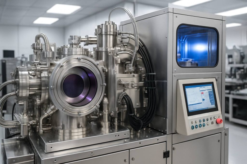
Extreme Ultraviolet (EUV) lithography equipment manufacturing represents a critical segment within the semiconductor fabrication industry, enabling the production of advanced integrated circuits at sub-7nm process nodes. EUV lithography utilizes light with a wavelength of 13.5 nanometers, allowing for significantly finer patterning compared to traditional deep ultraviolet (DUV) methods. This technology is essential for meeting the escalating demand for higher performance and energy-efficient chips in applications such as artificial intelligence, 5G, and high-performance computing.
As of 2025, the global EUV lithography equipment market is characterized by robust growth, driven by aggressive investments from leading foundries and integrated device manufacturers (IDMs). The market is highly consolidated, with ASML Holding N.V. maintaining a near-monopoly as the sole supplier of commercial EUV lithography systems. The company’s EUV systems are integral to the advanced manufacturing roadmaps of major semiconductor players, including Taiwan Semiconductor Manufacturing Company (TSMC), Samsung Electronics, and Intel Corporation.
According to recent market analyses, the global EUV lithography equipment market is projected to reach a valuation of approximately USD 25 billion by 2025, expanding at a compound annual growth rate (CAGR) exceeding 20% from 2022 to 2025. This growth is underpinned by the transition to 3nm and 2nm process technologies, which require the precision and throughput offered by next-generation EUV tools. The Asia-Pacific region, led by Taiwan and South Korea, continues to dominate demand, accounting for over 70% of global EUV equipment shipments, reflecting the concentration of advanced semiconductor manufacturing capacity in these geographies (SEMI).
- Key market drivers include the proliferation of data-centric applications, the scaling limitations of DUV lithography, and government-backed initiatives to localize semiconductor supply chains.
- Challenges persist in the form of high capital expenditure, complex supply chains for critical components (such as light sources and photomasks), and geopolitical tensions impacting cross-border technology transfers.
- Ongoing R&D efforts focus on improving EUV system productivity, reducing defect rates, and developing high-NA (numerical aperture) EUV platforms to support future technology nodes (Gartner).
In summary, the EUV lithography equipment manufacturing market in 2025 is defined by rapid technological advancement, strategic investments, and a pivotal role in enabling the next generation of semiconductor devices.
Key Technology Trends in EUV Lithography Equipment
Extreme Ultraviolet (EUV) lithography equipment manufacturing is undergoing rapid technological evolution as the semiconductor industry pushes toward sub-5nm and even 2nm process nodes in 2025. EUV lithography, which utilizes a 13.5 nm wavelength light source, enables the production of smaller, more densely packed transistors, critical for advanced logic and memory chips. The following key technology trends are shaping the EUV lithography equipment landscape in 2025:
- High-NA EUV Systems: The transition from conventional 0.33 numerical aperture (NA) systems to high-NA (0.55 NA) EUV scanners is a pivotal trend. High-NA EUV tools, such as the EXE:5200 series from ASML Holding, offer improved resolution and process window, enabling patterning at 2nm and below. These systems require significant advancements in optics, mask technology, and resist materials.
- Pellicle and Mask Innovations: EUV mask defectivity and pellicle durability remain critical challenges. In 2025, manufacturers are deploying advanced pellicle materials with higher EUV transmittance and thermal stability, as well as defect inspection and repair tools, to ensure yield and reliability. Companies like HOYA Corporation and Shin-Etsu Chemical are at the forefront of these developments.
- Source Power Scaling: Increasing the EUV light source power is essential for higher throughput. In 2025, leading suppliers are delivering source power levels exceeding 500W, reducing wafer exposure times and improving productivity. Cymer, a subsidiary of ASML, continues to innovate in laser-produced plasma (LPP) source technology.
- Resist Material Advancements: The demand for higher sensitivity and lower line edge roughness in EUV resists is driving the development of new chemically amplified and metal-oxide resists. Tokyo Ohka Kogyo and JSR Corporation are leading suppliers introducing next-generation resist formulations tailored for high-NA EUV.
- Equipment Ecosystem Integration: The complexity of EUV lithography requires tight integration of metrology, inspection, and computational lithography tools. Companies such as KLA Corporation and Synopsys are providing advanced solutions for defect detection, process control, and simulation, supporting the ramp-up of EUV production lines.
These technology trends underscore the collaborative and multidisciplinary nature of EUV lithography equipment manufacturing in 2025, as the industry addresses technical barriers to enable next-generation semiconductor devices.
Competitive Landscape and Leading Manufacturers
The competitive landscape of the extreme ultraviolet (EUV) lithography equipment market in 2025 is characterized by high entry barriers, technological complexity, and a concentrated supplier base. The market is dominated by a handful of players, with ASML Holding NV maintaining a near-monopoly as the sole commercial supplier of EUV lithography systems. ASML’s EUV platforms are critical for advanced semiconductor manufacturing at nodes below 7nm, and the company’s technological leadership is underpinned by its proprietary light source technology, precision optics, and extensive intellectual property portfolio.
Other major players in the broader lithography equipment market, such as Canon Inc. and Nikon Corporation, have focused primarily on deep ultraviolet (DUV) systems and have not achieved commercial deployment of EUV tools as of 2025. Both companies continue to invest in R&D for next-generation lithography, but the technical and capital requirements for EUV have limited their market share in this segment.
Key semiconductor foundries and integrated device manufacturers (IDMs), including Taiwan Semiconductor Manufacturing Company (TSMC), Samsung Electronics, and Intel Corporation, are the primary customers for EUV equipment. These companies have formed strategic partnerships and long-term supply agreements with ASML to secure access to EUV tools, which are essential for producing leading-edge chips for applications in AI, 5G, and high-performance computing.
The supply chain for EUV systems is highly specialized, involving critical component suppliers such as Carl Zeiss AG (optics), Cymer (a division of ASML) (light sources), and TRUMPF Group (laser technology). These suppliers play a pivotal role in enabling ASML’s production capacity and innovation pipeline.
Geopolitical factors and export controls, particularly between the US, EU, and China, continue to shape the competitive dynamics. Restrictions on the sale of advanced EUV systems to certain regions have reinforced ASML’s strategic importance and limited the emergence of new competitors. As of 2025, no Chinese manufacturer has achieved commercial-scale EUV lithography capability, though significant investments and government support are being directed toward domestic development.
Overall, the EUV lithography equipment market in 2025 remains highly consolidated, with ASML at the forefront, supported by a network of specialized suppliers and a customer base of leading-edge chipmakers driving demand for ever-smaller process nodes.
Market Growth Forecasts (2025–2030): CAGR, Revenue, and Volume Analysis
The extreme ultraviolet (EUV) lithography equipment manufacturing market is poised for robust growth between 2025 and 2030, driven by escalating demand for advanced semiconductor devices and the ongoing transition to sub-5nm process nodes. According to projections from Gartner and SEMI, the global EUV lithography equipment market is expected to register a compound annual growth rate (CAGR) of approximately 18–22% during this period. This acceleration is underpinned by aggressive capital expenditures from leading foundries and integrated device manufacturers (IDMs), particularly in Asia-Pacific and North America.
Revenue forecasts indicate that the EUV lithography equipment market, valued at around $8.5 billion in 2024, could surpass $19 billion by 2030. This surge is attributed to the increasing adoption of EUV systems for high-volume manufacturing of logic and memory chips, as well as the expansion of EUV capacity by major players such as TSMC, Samsung Electronics, and Intel. The market’s volume growth is also notable, with annual shipments of EUV scanners projected to rise from approximately 60 units in 2025 to over 120 units by 2030, as reported by ASML Holding, the dominant supplier in this segment.
- Regional Dynamics: Asia-Pacific is expected to maintain its leadership, accounting for over 60% of global EUV equipment demand, fueled by aggressive fab expansions in Taiwan, South Korea, and China. North America will also see significant growth, driven by U.S. government incentives and domestic chip manufacturing initiatives.
- Technology Trends: The transition to high-NA (numerical aperture) EUV systems, anticipated to begin in 2025–2026, will further boost market value and shipment volumes, as chipmakers seek to enable even smaller process geometries and higher yields.
- Revenue Concentration: The market remains highly consolidated, with ASML Holding capturing over 90% of global EUV lithography equipment revenues, underscoring the strategic importance of supply chain resilience and technology leadership.
In summary, the 2025–2030 period will be characterized by double-digit CAGR, significant revenue expansion, and rising shipment volumes, positioning EUV lithography equipment manufacturing as a critical enabler of next-generation semiconductor innovation.
Regional Market Analysis: North America, Europe, Asia-Pacific, and Rest of World
The global market for extreme ultraviolet (EUV) lithography equipment is characterized by significant regional disparities in manufacturing capabilities, adoption rates, and strategic investments. In 2025, North America, Europe, Asia-Pacific, and the Rest of the World (RoW) each play distinct roles in the EUV lithography landscape, shaped by their respective semiconductor industries, government policies, and supply chain dynamics.
- North America: The United States remains a pivotal player in the EUV lithography equipment market, primarily through its dominance in semiconductor design and critical component supply. While the U.S. does not manufacture complete EUV systems, it is home to key suppliers of photomasks, light sources, and advanced materials. Strategic government initiatives, such as the CHIPS and Science Act, are expected to bolster domestic semiconductor manufacturing and indirectly stimulate demand for EUV equipment in 2025. However, the region remains reliant on European and Asian partners for full-system integration and deployment (Semiconductor Industry Association).
- Europe: Europe, led by the Netherlands-based ASML Holding, is the undisputed global leader in EUV lithography equipment manufacturing. ASML is the sole supplier of commercial EUV systems, and its production capacity is a critical bottleneck for the global semiconductor industry. In 2025, Europe’s strategic focus is on expanding ASML’s output and securing the supply chain for high-precision components, such as optics from Carl Zeiss AG. The European Union’s Chips Act further supports regional R&D and manufacturing, aiming to strengthen Europe’s position in advanced semiconductor technologies (European Commission).
- Asia-Pacific: The Asia-Pacific region, particularly Taiwan, South Korea, and Japan, is the largest consumer of EUV lithography equipment, driven by the aggressive technology roadmaps of foundries like TSMC and Samsung Electronics. These companies are at the forefront of sub-5nm and 3nm chip production, necessitating substantial investments in EUV tools. Japan also plays a vital role in supplying photoresists and other critical materials. Regional governments are incentivizing local manufacturing and R&D to reduce dependence on foreign technology (SEMI).
- Rest of World: Other regions, including China, are rapidly increasing investments in EUV-related R&D and infrastructure. However, access to EUV systems is constrained by export controls and technology transfer restrictions imposed by the U.S. and its allies. As a result, local efforts are focused on developing indigenous alternatives and strengthening upstream supply chains (Brookings Institution).
In summary, while Europe dominates EUV equipment manufacturing, North America and Asia-Pacific are critical in the supply chain and end-use, respectively. Geopolitical factors and supply chain resilience will continue to shape regional dynamics in 2025.
Future Outlook: Innovation, Investments, and Emerging Applications
The future outlook for extreme ultraviolet (EUV) lithography equipment manufacturing in 2025 is characterized by robust innovation, significant capital investments, and the emergence of new applications that are set to redefine the semiconductor landscape. As the industry pushes toward sub-2nm process nodes, EUV technology remains indispensable for enabling higher transistor densities and improved chip performance. Leading manufacturers are intensifying their R&D efforts to enhance EUV source power, improve mask defectivity control, and increase throughput, all of which are critical for meeting the stringent requirements of next-generation logic and memory devices.
Investment in EUV infrastructure is accelerating, with major foundries and integrated device manufacturers (IDMs) allocating substantial budgets for EUV tool procurement and fab upgrades. For instance, TSMC and Samsung Electronics have announced multi-billion-dollar capital expenditures focused on expanding their EUV capacity, aiming to secure leadership in advanced process technologies. Equipment suppliers, most notably ASML Holding, are scaling up production of their latest EUV systems, such as the Twinscan NXE and EXE series, to meet surging demand from global chipmakers.
Emerging applications are also shaping the future of EUV lithography. Beyond traditional high-performance computing and mobile processors, EUV is increasingly being adopted for advanced DRAM and NAND flash memory production, as well as for specialized chips in artificial intelligence (AI), automotive, and 5G infrastructure. The adoption of high-NA (numerical aperture) EUV systems, expected to ramp up in 2025, will further enable patterning at even smaller geometries, unlocking new possibilities for chip design and integration.
- Continued innovation in EUV source technology is expected to drive higher productivity and lower cost per wafer, making EUV more accessible for a broader range of semiconductor applications.
- Strategic partnerships and consortia, such as those led by SEMI and imec, are fostering collaborative research to address technical challenges and accelerate ecosystem readiness for high-volume EUV manufacturing.
- Geopolitical factors and supply chain resilience are prompting regional investments in EUV tool manufacturing and component sourcing, particularly in the US, Europe, and East Asia.
Overall, 2025 is poised to be a pivotal year for EUV lithography equipment manufacturing, with innovation, investment, and application diversification driving the next wave of semiconductor industry growth.
Challenges and Opportunities: Supply Chain, Cost Pressures, and Regulatory Factors
The manufacturing of Extreme Ultraviolet (EUV) lithography equipment in 2025 faces a complex landscape shaped by supply chain vulnerabilities, escalating cost pressures, and evolving regulatory frameworks. These factors collectively influence the pace of innovation, production scalability, and the global competitive balance in the semiconductor industry.
Supply Chain Challenges: EUV lithography systems are among the most intricate machines ever built, requiring thousands of precision components sourced globally. The supply chain for critical parts—such as high-reflectivity mirrors, light sources, and photomasks—remains highly concentrated, with a few specialized suppliers dominating the market. Disruptions, whether from geopolitical tensions, natural disasters, or logistics bottlenecks, can significantly delay production timelines. For instance, the reliance on ASML Holding NV for EUV systems and on a handful of suppliers for key subsystems has exposed the industry to single points of failure, as highlighted during the COVID-19 pandemic and subsequent semiconductor shortages.
Cost Pressures: The capital intensity of EUV equipment manufacturing is immense. Each EUV scanner can cost upwards of $150 million, with R&D and precision engineering driving up expenses. The need for continuous innovation to achieve finer process nodes (e.g., 3nm and below) further escalates costs. Manufacturers are under pressure to balance these investments with the demand for affordable chips, especially as end markets like automotive and consumer electronics seek cost-effective solutions. According to SEMI, the average capital expenditure for leading-edge fabs is expected to rise by over 10% annually through 2025, largely due to EUV adoption.
Regulatory Factors: Export controls and technology transfer restrictions are increasingly shaping the EUV landscape. The U.S., Japan, and the Netherlands have imposed tighter regulations on the export of advanced lithography equipment to certain countries, notably China, citing national security concerns. These measures, as reported by U.S. Bureau of Industry and Security, limit market access for EUV manufacturers and complicate global supply chains. At the same time, environmental regulations regarding energy consumption and hazardous materials in manufacturing processes are prompting equipment makers to invest in greener technologies and compliance systems.
Opportunities: Despite these challenges, opportunities abound. The push for domestic semiconductor manufacturing in the U.S., Europe, and Asia is driving new investments in EUV-capable fabs. Collaborative R&D initiatives and government incentives, such as those under the U.S. CHIPS Act and the European Chips Act, are fostering innovation and supply chain resilience. Additionally, advances in component miniaturization and process automation offer pathways to cost reduction and efficiency gains.
Sources & References
- ASML Holding N.V.
- HOYA Corporation
- Shin-Etsu Chemical
- Tokyo Ohka Kogyo
- JSR Corporation
- KLA Corporation
- Synopsys
- Canon Inc.
- Nikon Corporation
- Carl Zeiss AG
- TRUMPF Group
- Semiconductor Industry Association
- European Commission
- Brookings Institution
- imec
- U.S. Bureau of Industry and Security


